Enhanced functionality for WaveAnalyzer family
The upcoming release of the GUI version 1.8 adds significant functions and improvements to the WaveAnalyzer family:
Optical Signal to Noise Ratio (OSNR)
Sequential Measuring has been added to the OSNR measurement methods. This allows measuring of the OSNR value using in-band noise. Inband noise is obtained by a separate measurement in which the channel is switched off (or moved to a different frequency) and only the noise remains in the spectral window of interest. The channel with the signal present is then measured in a separate step. The benefit of this method is that the true noise in the channel is considered for the OSNR, and not an estimated noise level derived from measurements outside the channel.
The WaveAnalyzer GUI package also provides warning messages in case the user launches excessive power levels to the instrument. Such power levels can severely compromise the accuracy in particular of OSNR measurements.
Side Mode Suppression Ratio (SMSR)
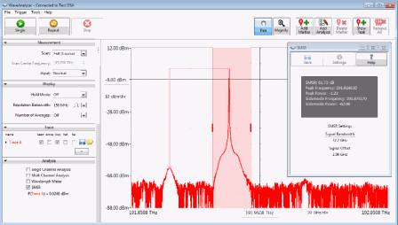
The new GUI version 1.8 allows the measurement of the SMSR of narrowband (laser) sources. The algorithm identifies the largest side mode,

provides provides the SMSR value and displays the result in an intuitive manner, as seen in the screenshot above.
The WaveAnalyzer GUI version 1.8 is scheduled for release at the end of October. Contact waveanalyzer@finisar.com if you would like to test the beta package prior to release.
Download the latest released software and firmware from the Optical
Instrumentation Webpages.
New Product: Ultra-high RF Output Power Detectors
Finisar’s series of high RF output power detectors is now extended with the addition of the new
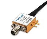
VPDV2120 compact and hermetically packaged, optical detector module.

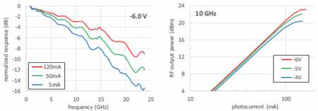
The VPDV2120, which is currently introduced, provides ultra-high RF saturation output power of >22 dBm (150 mA) at a frequency of 10 GHz. It offers a high responsivity of 0.55 A/W (1550 nm) with high linearity (typical OIP3 values above 30 dBm at a frequency of 10 GHz) and does not require cooling. The device uses a modified uni-travelling carrier (MUTC) photodetector chip.
The VPDV2120 (Order Code VPDV2120-VF-FA) is not matched to 50 Ω and requires a bias voltage of -6 V, for which an external Bias-Tee (Order Code EVAL KIT VPDV) can also be ordered.

Finisar’s HPDV2120 provides a high RF output power; it is in production and can be ordered now (order code HPDV2120-VF-FA). The HPDV is a compact module based on an advanced waveguide photodetector chip integrated with a Bias-Tee.
The module utilizes a mode-converting tapered waveguide for efficient fiberto- chip coupling and a 1×4 Multi-Mode Interference (MMI) Coupler. The optical signal is split by the MMI coupler into four equal parts and then it is fed into an array of four photodiodes which are connected in-parallel. It has a responsivity of 0.52 A/W @ 1550 nm and a high saturation photocurrent of 35 mA @ 20 GHz. The module is capable of delivering 6 dBm RF output power @ 20 GHz and 3 dBm @ 50 GHz. The device exhibits high linearity with typical OIP3 values above 20 dBm at a frequency of 40 GHz.
Finisar is now offering prototypes of our well-known 70 GHz single and balanced detectors with dual wavelength capabilities, supporting activities in the O-band (1310 nm). Finisar received several inquiries for these products and is now taking orders for prototypes of the first generation XPDV33xx (single PD) and BPDV33xx (balanced PD modules).
The VPDV2120 (Order Code VPDV2120-VF-FA) is not matched to 50 Ω and requires a bias voltage of -6 V, for which an external Bias-Tee (Order Code EVAL KIT VPDV) can also be ordered.
Diffractive Optical Elements for Sensing
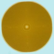
Finisar manufactures all-dielectric Diffractive Optical Elements (DOE) fabricated by Deep UltraViolet (DUV) photolithography patterning process.

These products are intended for use in demanding industrial and consumer applications, such as 3D sensing and telecommunications. Micron-thick active phase-transforming layer is directly etched into hard dielectric oxides on robust fused silica substrate. Organics-free material platform is characterized by excellent reliability and can withstand high optical power and extreme temperatures up to 500°C.
DOE are now commercially available and may collimate or focus light, or otherwise transform incoming wavefront. Complex aberration-corrective aspheric focusing, off-axis or extended source collimation phase function are rendered using continuous phase rendition technique on a 500 nm spatial grid. Multiple phase transformation functions (such as top hat generators, phase converters, computer-generated holograms and optical taps) may be combined in a single active layer.
